
How a solvent-free lithography method could transform the future of delicate electronics
When Fabrication Becomes the Problem
Why can manufacturing damage the very materials it tries to build?
In the world of advanced electronics, the frontier of innovation is measured in atoms. Engineers and physicists now design devices from materials so thin they can be counted in layers of molecules, sometimes only a few atoms thick. These materials promise faster processors, flexible electronics, ultra-sensitive sensors, and entirely new forms of computing.
Yet a quiet paradox sits at the center of this progress: the very materials that could power the next generation of devices are often too fragile for the manufacturing processes used to build them.
Traditional semiconductor fabrication relies heavily on photolithography, a technique that patterns microscopic circuits onto materials using chemical photoresists, solvents, and multiple wet-processing steps. For decades this system has powered the evolution of modern electronics.
However, many emerging materials such as perovskites, black phosphorus, and two-dimensional semiconductors are extremely sensitive to chemical exposure. Solvents can oxidize surfaces, leave residues, or destabilize atomic structures. Oxygen exposure may degrade layered crystals, while even mild cleaning processes can introduce defects.
In other words, the industrial tools that built the digital age may be too harsh for the materials that could define its future.

A New Approach: The Selenium Mediator
How can lithography work without chemical solvents?
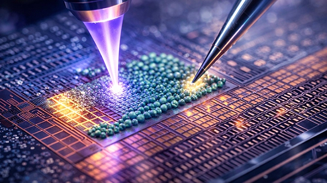
A study published in Nature Communications (2026) proposes a radically different strategy: remove solvents from the lithography process altogether.
Researchers developed an all-dry lithography method that uses a thin layer of selenium molecules as a temporary mediator during patterning.
Instead of coating surfaces with polymer photoresists and chemical developers, engineers deposit a nanoscale selenium film that performs two key roles.
First, the selenium layer enables precise pattern transfer, allowing microscopic structures to be defined during lithography. Second, it acts as a protective barrier that shields delicate materials from chemical exposure.
After patterning is complete, the selenium layer can be removed mechanically, leaving a clean surface and an intact device structure.
Because the process avoids liquid solvents and wet chemical treatments, it represents a rare form of fully dry microfabrication.

Why Dry Fabrication Matters
What problems do solvents create at the nanoscale?
At atomic scales, contamination is not a minor inconvenience. Even extremely small amounts of residue can disrupt how electronic devices behave.
Chemical remnants trapped on a semiconductor surface may alter electron transport, change optical properties, or introduce defects that degrade device performance.
Many emerging electronic materials rely on extremely precise electronic interactions. Even tiny impurities can destroy the properties researchers are trying to harness.
By eliminating wet processing steps, the selenium-mediated technique dramatically reduces opportunities for contamination while preserving fragile surfaces.
Laboratory experiments showed that researchers could successfully pattern sensitive materials without damaging their electronic properties. Importantly, the method also demonstrated compatibility with wafer-scale fabrication, meaning it could potentially integrate with existing semiconductor manufacturing systems.
For engineers attempting to transform laboratory discoveries into industrial technologies, this compatibility is critical.

Enabling the Next Generation of Devices
What technologies could benefit from solvent-free lithography?
If the selenium-mediated technique proves scalable, it could accelerate progress across multiple emerging technologies.
Flexible electronics are one of the most promising applications. Ultra-thin semiconductors capable of bending and stretching could benefit from fabrication methods that avoid harsh chemical processing. These materials may eventually power wearable sensors, foldable displays, and implantable medical devices.
Environmental and biomedical sensors could also gain advantages. Many sensing materials require extremely clean surfaces to detect subtle chemical or biological signals. Reducing contamination during fabrication may significantly improve their sensitivity.
Photonic devices represent another frontier. Materials used in lasers, telecommunications systems, and quantum photonics often degrade when exposed to conventional lithography chemicals. Dry fabrication may help preserve their optical performance.
Perhaps most intriguing is the potential for quantum materials. These atomically thin systems are notoriously sensitive to fabrication damage. A gentler lithography technique could allow researchers to build experimental quantum devices that were previously impossible to manufacture reliably.

A Greener Path for Chip Manufacturing
Can solvent-free fabrication make semiconductor production more sustainable?
Conventional semiconductor manufacturing consumes large quantities of organic solvents and chemical photoresists. These materials require complex waste-management systems and generate significant chemical by-products.
An all-dry lithography approach could reduce chemical consumption and simplify parts of the clean-room infrastructure.
Although the selenium-based technique is still at the research stage, it highlights a broader trend in materials science: developing manufacturing methods that combine atomic-scale precision with environmental responsibility.
In an industry increasingly focused on sustainability, innovations in fabrication processes may prove just as important as the devices they help create.

❓ Frequently Asked Questions (FAQ)
Why are emerging semiconductor materials so fragile during manufacturing?
Many next-generation materials are only a few atoms thick and extremely sensitive to chemical exposure. Traditional lithography uses solvents and photoresists that can oxidize surfaces or leave residues. These contaminants can disrupt the electronic properties that make the materials valuable.
What is selenium-mediated lithography?
It is a solvent-free fabrication method where a thin layer of selenium molecules temporarily acts as a patterning mediator and protective barrier. After the lithography process is complete, the selenium layer can be removed mechanically, leaving a clean surface.
Why is dry fabrication important for nanotechnology?
At nanoscale dimensions, even trace chemical contamination can alter electrical or optical behavior. Dry fabrication minimizes chemical exposure and helps preserve delicate material structures.
Could this method work in large semiconductor factories?
Early experiments show that the technique can operate on wafer-scale samples, suggesting potential compatibility with existing semiconductor manufacturing systems. However, further research and industrial testing are needed before large-scale adoption.
Does solvent-free chip fabrication help the environment?
Potentially yes. Reducing solvent use in semiconductor fabrication could decrease chemical waste, simplify waste-treatment systems, and reduce the environmental footprint of chip manufacturing.
References
Nature Communications (2026). Research on solvent-free lithography using selenium mediator.
Sze, S. M., & Ng, K. K. (2006). Physics of Semiconductor Devices. Wiley.
International Technology Roadmap for Semiconductors (ITRS). Semiconductor manufacturing processes.
Key Takeaways
- How a solvent-free lithography method could transform the future of delicate electronics
- Engineers and physicists now design devices from materials so thin they can be counted in layers of molecules, sometimes only a few atoms thick.
- Yet a quiet paradox sits at the center of this progress: the very materials that could power the next generation of devices are often too fragile for the manufacturing processes used to build them.
- However, many emerging materials such as perovskites, black phosphorus, and two-dimensional semiconductors are extremely sensitive to chemical exposure.
- Oxygen exposure may degrade layered crystals, while even mild cleaning processes can introduce defects.
Frequently Asked Questions
When Fabrication Becomes the Problem?
In the world of advanced electronics, the frontier of innovation is measured in atoms. Engineers and physicists now design devices from materials so thin they can be counted in layers of molecules, sometimes only a few atoms thick. These materials promise faster processors, flexible electronics, ult
Why can manufacturing damage the very materials it tries to build?
In the world of advanced electronics, the frontier of innovation is measured in atoms. Engineers and physicists now design devices from materials so thin they can be counted in layers of molecules, sometimes only a few atoms thick. These materials promise faster processors, flexible electronics, ult
What should you know about a New Approach: The Selenium Mediator?
A study published in Nature Communications (2026) proposes a radically different strategy: remove solvents from the lithography process altogether.
How can lithography work without chemical solvents?
A study published in Nature Communications (2026) proposes a radically different strategy: remove solvents from the lithography process altogether.
Why Dry Fabrication Matters?
At atomic scales, contamination is not a minor inconvenience. Even extremely small amounts of residue can disrupt how electronic devices behave.